FUJITSU: Hardware Challenges in Superconducting FTQC
Yoshiyasu Doi, Senior Research Director
Fujitsu Research Quantum Lab
2026.04.02 · updated 2026.10.03FUJITSU is a Japanese manufacturer and developer of full-stack quantum computers. It collaborates closely with the RIKEN Center for Quantum Computing in Japan, with the goal of developing a fault-tolerant quantum computer (FTQC) designed and built domestically in Japan. This talk mainly introduced and assessed the challenges that must be addressed on the path toward the practical realization of large-scale FTQC.
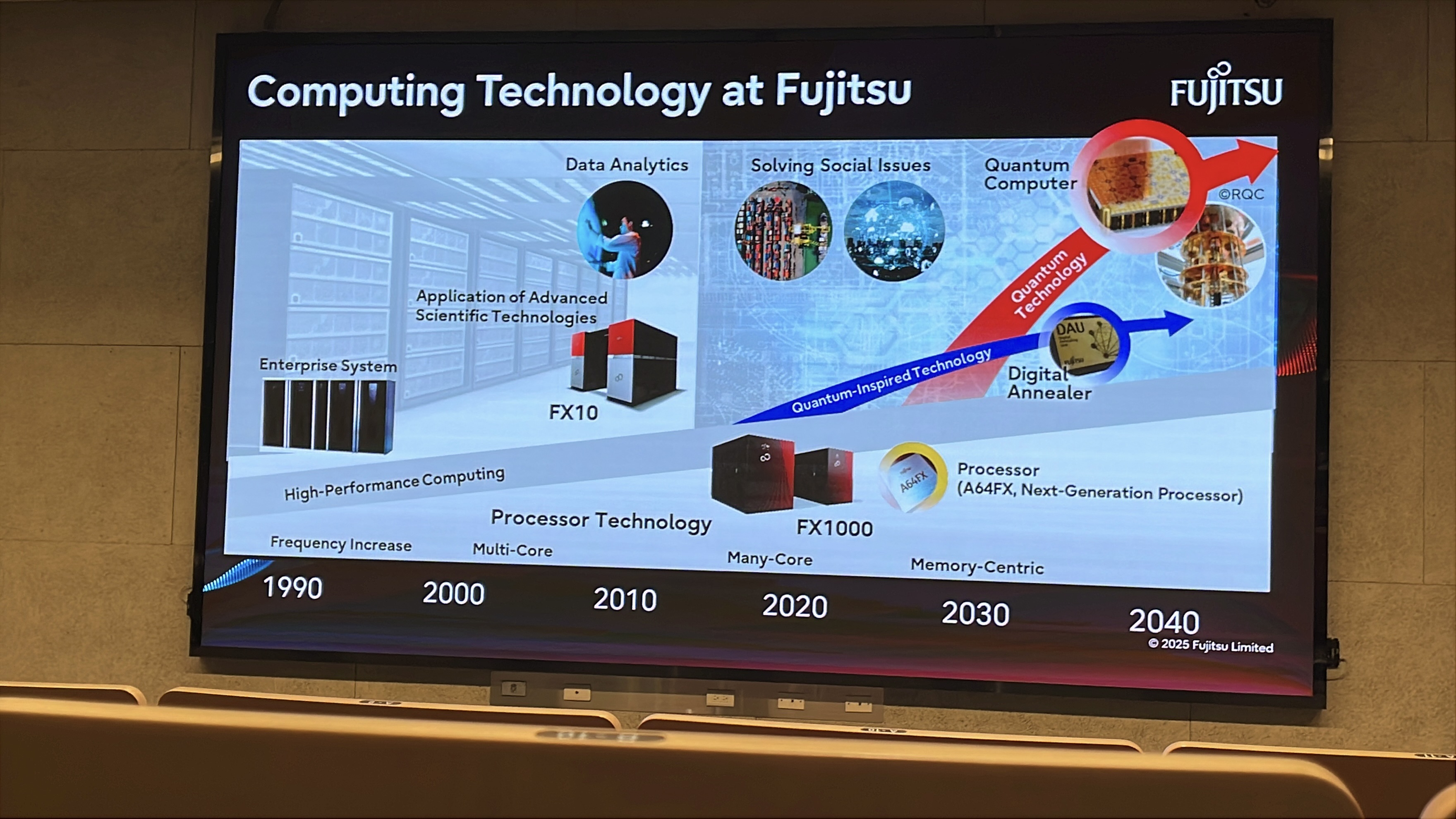
▲ FUJITSU has enterprise-level data center and supercomputing center deployment solutions in Japan. Interestingly, the slide below mentions the ways FUJITSU has improved computational power at different stages:
Higher clock frequency: through high-frequency CPU operation
Multi-core computing: multi-core CPUs
Many-core computing: using more processing cores to increase parallelism
Memory-centric architecture: improving data movement, bandwidth, and coordination between memory and processing cores.
In addition, FUJITSU is also investing in the computational development of next-generation quantum technologies and quantum-inspired technologies.
Types of Quantum Computers
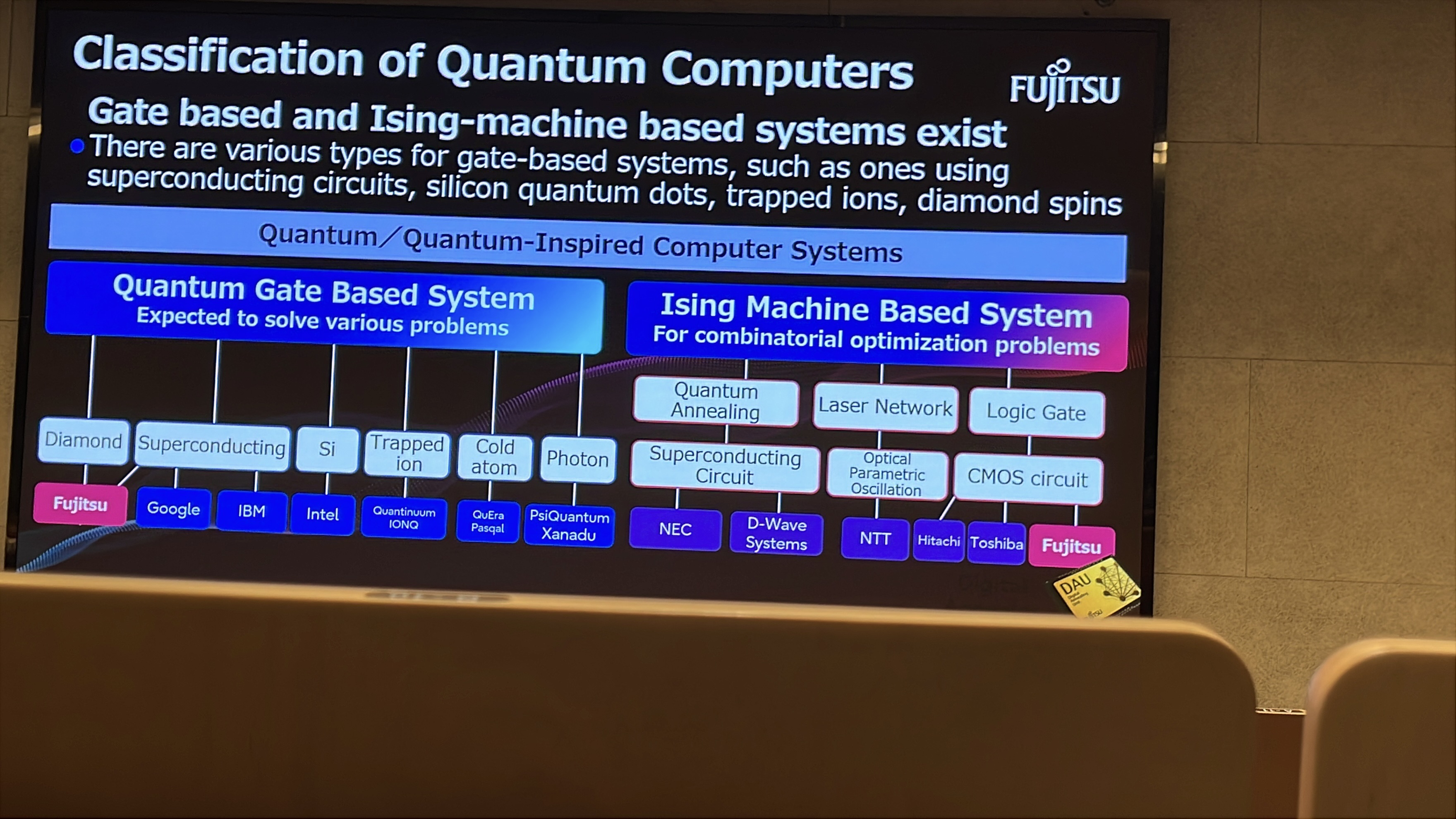
▲ This slide places quantum gate-based systems beside Ising machines for combinatorial optimization. The latter category includes both quantum annealers and classical CMOS implementations. An Ising machine does not necessarily exploit quantum effects, and Fujitsu's Digital Annealer should not be treated as a universal gate-based quantum computer.
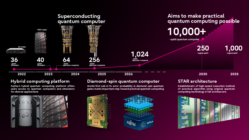
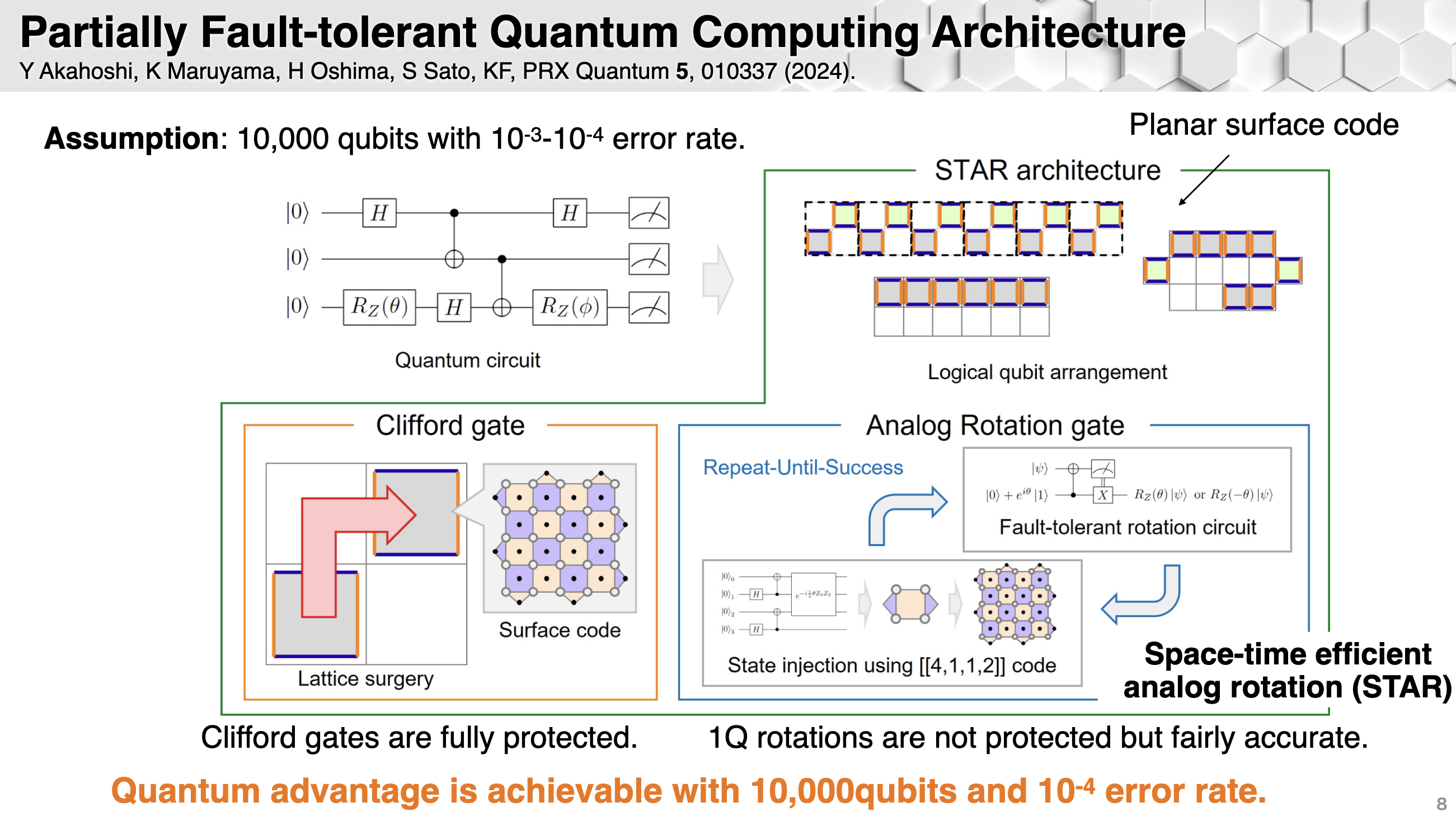
▲ FUJITSU's quantum computer roadmap. FUJITSU's research includes superconducting quantum computers and diamond spin quantum computers. STAR stands for Space-Time efficient Analog Rotation. It combines error-corrected Clifford gates with direct analog rotations to reduce resource requirements for early-FTQC. The rotations retain residual errors; partial fault tolerance does not mean that every operation is fully protected. [Original STAR paper]
Ref: https://global.fujitsu/en-global/technology/research/quantum
Ref: https://global.fujitsu/-/media/Project/Fujitsu/Fujitsu-HQ/technology/research/quantum/event-202503/FQD2025japan_guest_talk3.pdf
FUJITSU and RIKEN Multi-Qubit System Development
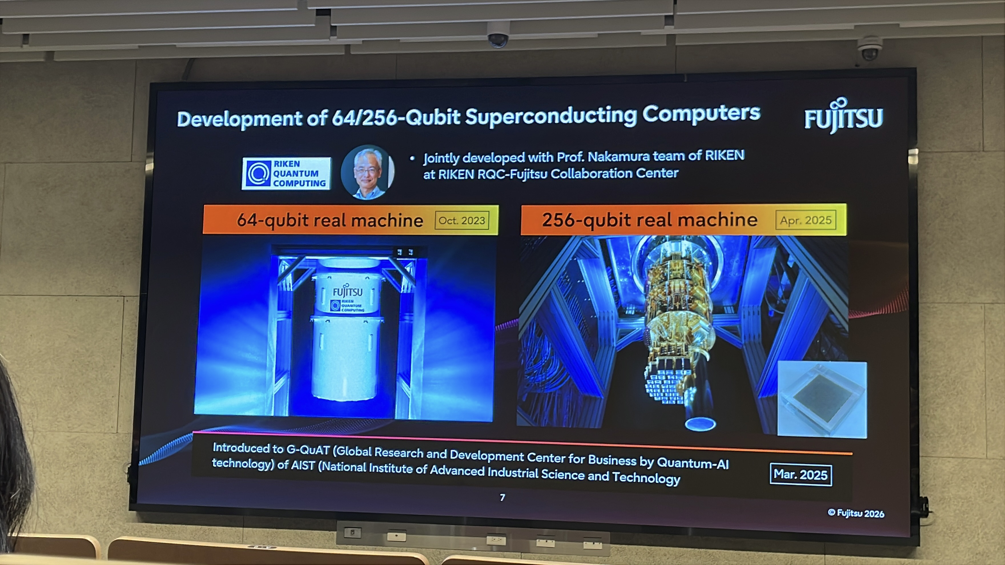
▲ FUJITSU is collaborating with Yasunobu Nakamura, the leader of the RIKEN quantum computing center, to develop multi-qubit systems.
Scaling this system requires the chip, packaging, cryogenic wiring, and control electronics to evolve together. The transmon follows the charge-qubit design lineage; flux qubits are a distinct superconducting circuit family and should not all be described as direct transmon predecessors.
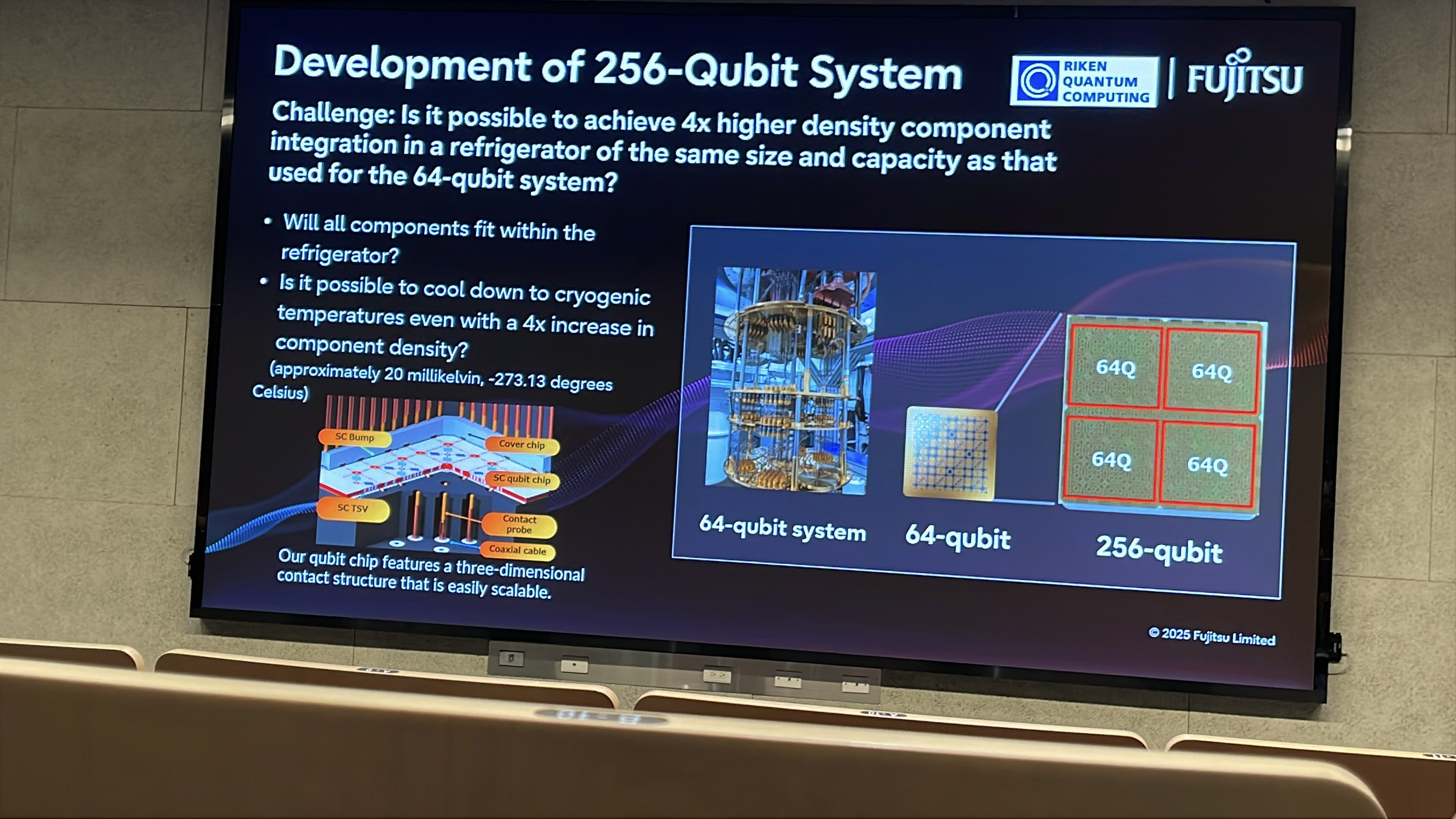
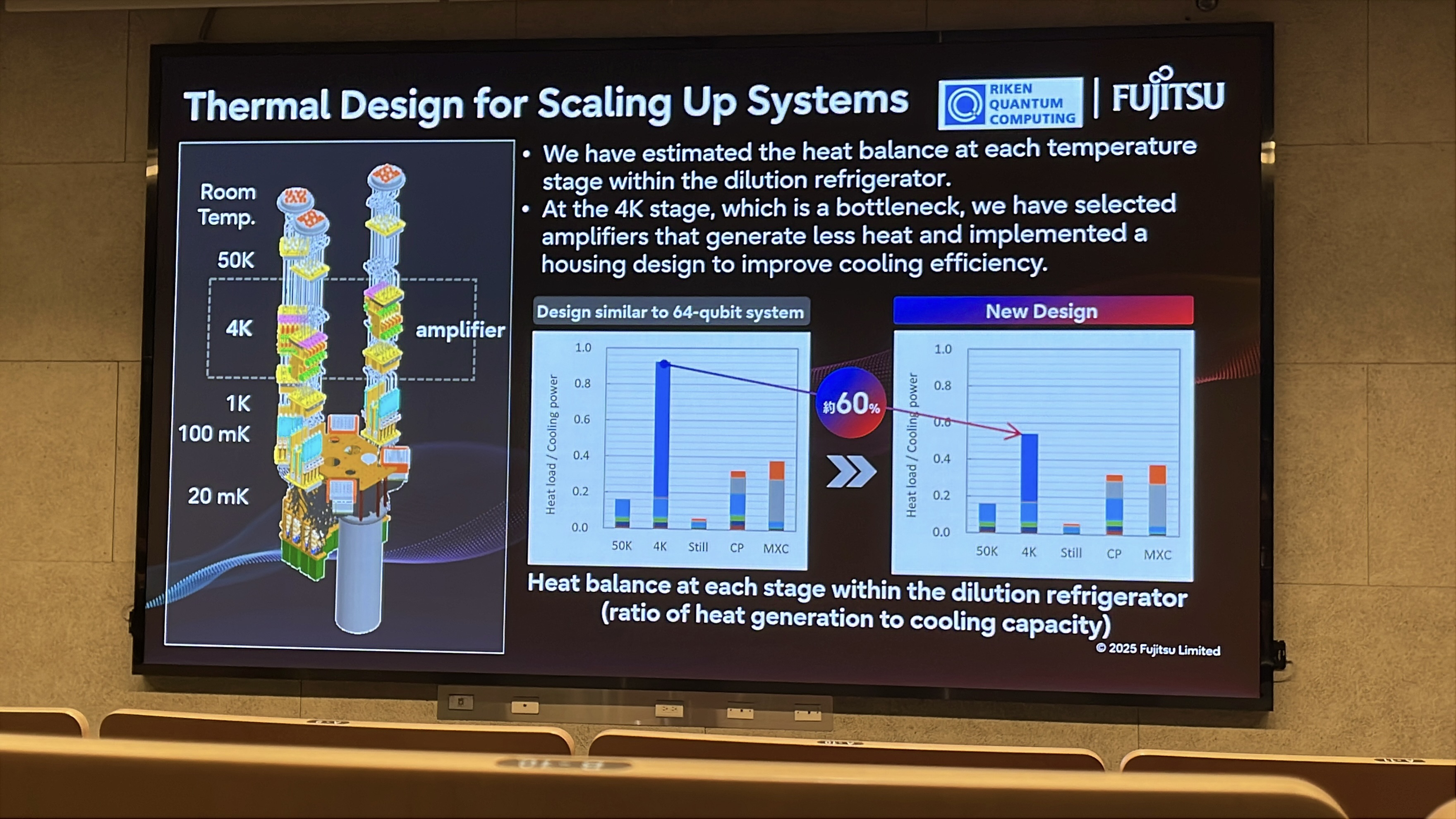
▲ Fujitsu and RIKEN announced their 256-qubit system in April 2025. This slide explains the extension of the unit-cell layout and three-dimensional wiring approach established for the 64-qubit system, together with denser packaging and improved thermal design. It does not mean simply joining four separate quantum computers. [RIKEN announcement]
Large-Area Superconducting Circuit Panels and Qubit Variability
The fabrication of multi-qubit chips is in fact similar to the semiconductor wafer industry: a large number of quantum circuits are integrated on large-area wafers. The related issues of mass production therefore involve the uniformity of qubits across the wafer. Because quantum response is extremely sensitive and Josephson junctions require very high process precision, the properties of superconducting qubits distributed across a wafer do in practice vary to some extent. Post-processing can tune the qubits toward their respective design targets.
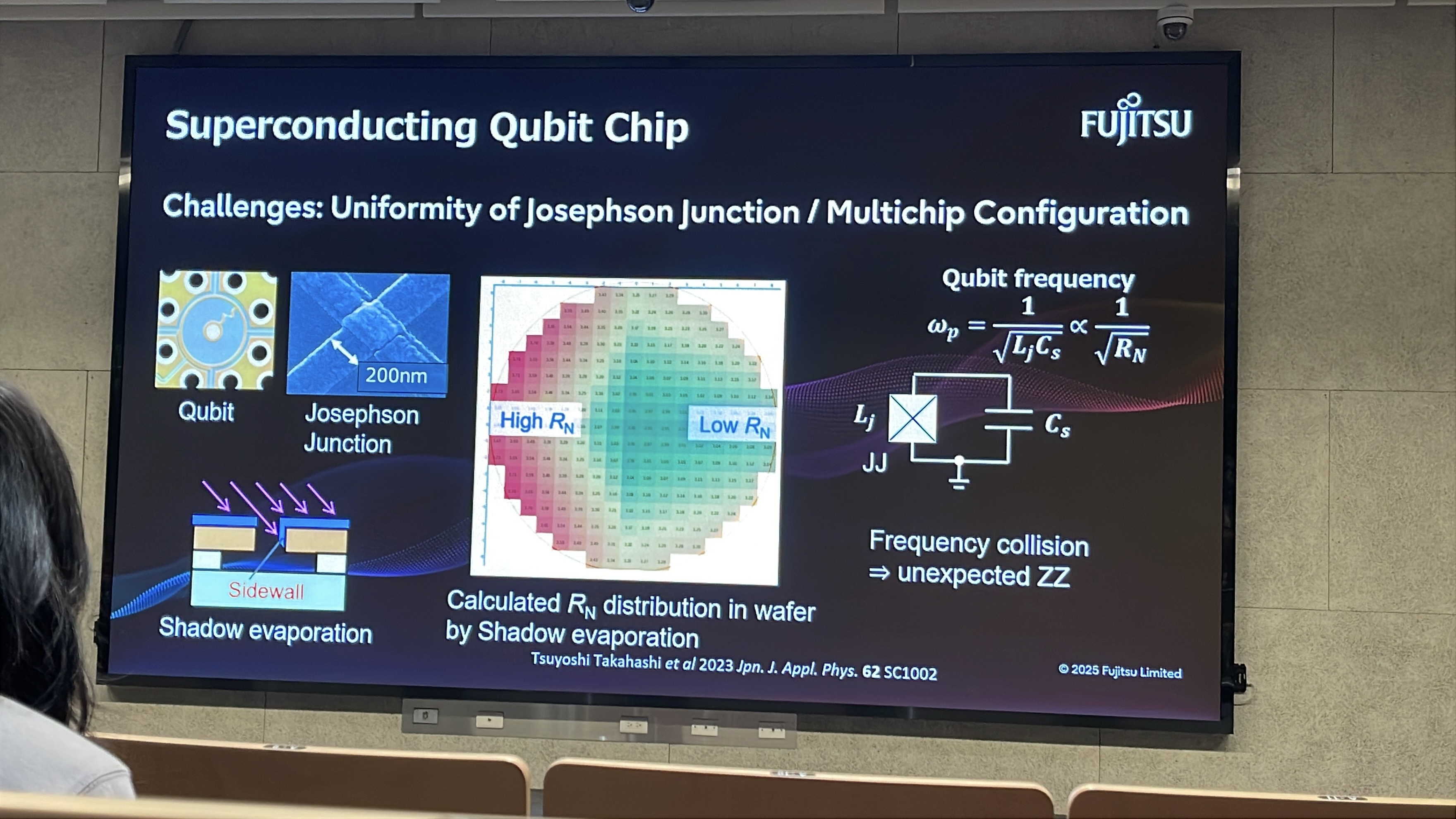
▲ This figure shows position-dependent variations in junction geometry and normal-state resistance produced by shadow evaporation, including sidewall deposition effects. Junction resistance is related to qubit frequency. Deviations from the frequency plan can cause frequency collisions and unwanted ZZ interactions, making fabrication uniformity and subsequent frequency adjustment important.
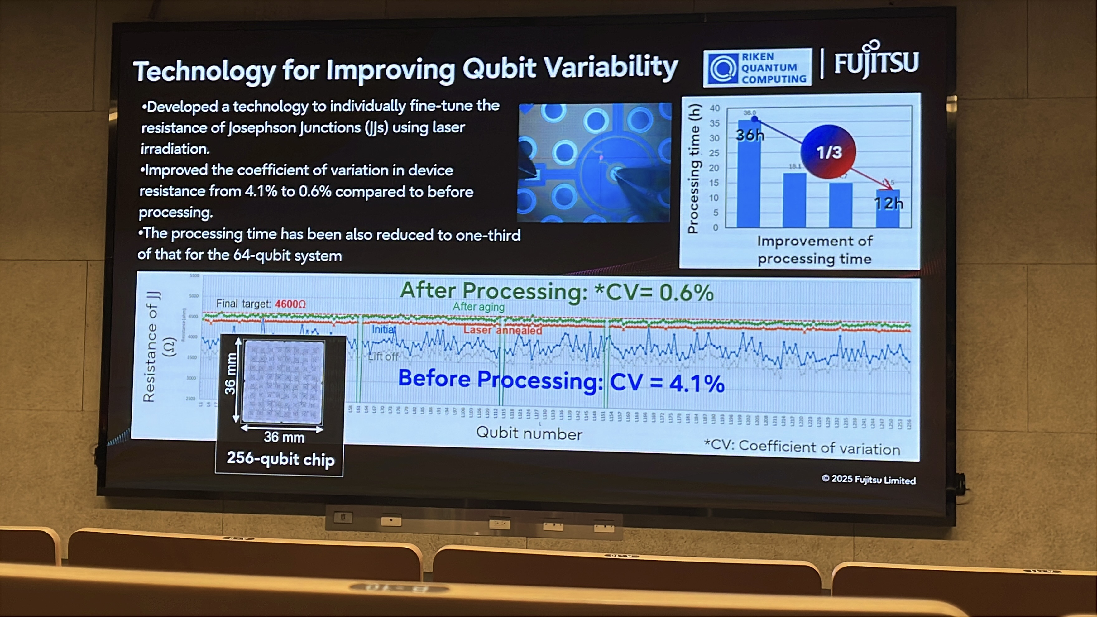
▲ RIKEN and Fujitsu use laser annealing to adjust Josephson-junction resistance. Probes measure the junction resistance at room temperature, and local laser heating brings it closer to the target. The slide reports a reduction in the resistance coefficient of variation from 4.1% to 0.6%. This measures junction-resistance uniformity; qubit frequencies and gate performance still require cryogenic validation.
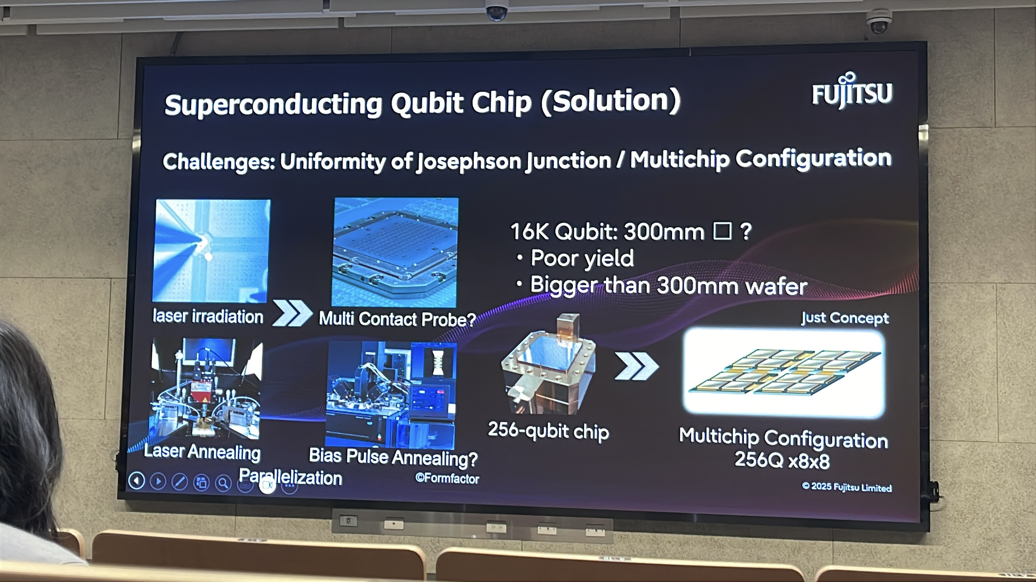
▲ However, when moving toward larger numbers of qubits, measuring each qubit individually and aligning a laser for local heating may not be a method that scales rapidly.
The slide proposes multi-contact probes and bias-pulse annealing as possible routes to parallelization, marking both with question marks. These are directions for exploring more efficient junction adjustment; the slide does not establish their implementation details or completed validation results.
Infrastructure Scale of a Quantum Computing Center
Practical quantum computing depends on the algorithm's logical-qubit count, circuit depth, and acceptable failure probability. There is no fixed conversion between physical and logical qubits: the code, hardware error rates, connectivity, and target logical error rate determine the resources required.
The talk contrasts early-FTQC scenarios with roughly 10,000–60,000 physical qubits and longer-term million-qubit scenarios. These are estimates under particular architectural and application assumptions, not universal thresholds for quantum advantage. For engineers, a central question is whether control channels, cryogenic heat loads, connectors, and racks remain manageable as the processor grows.
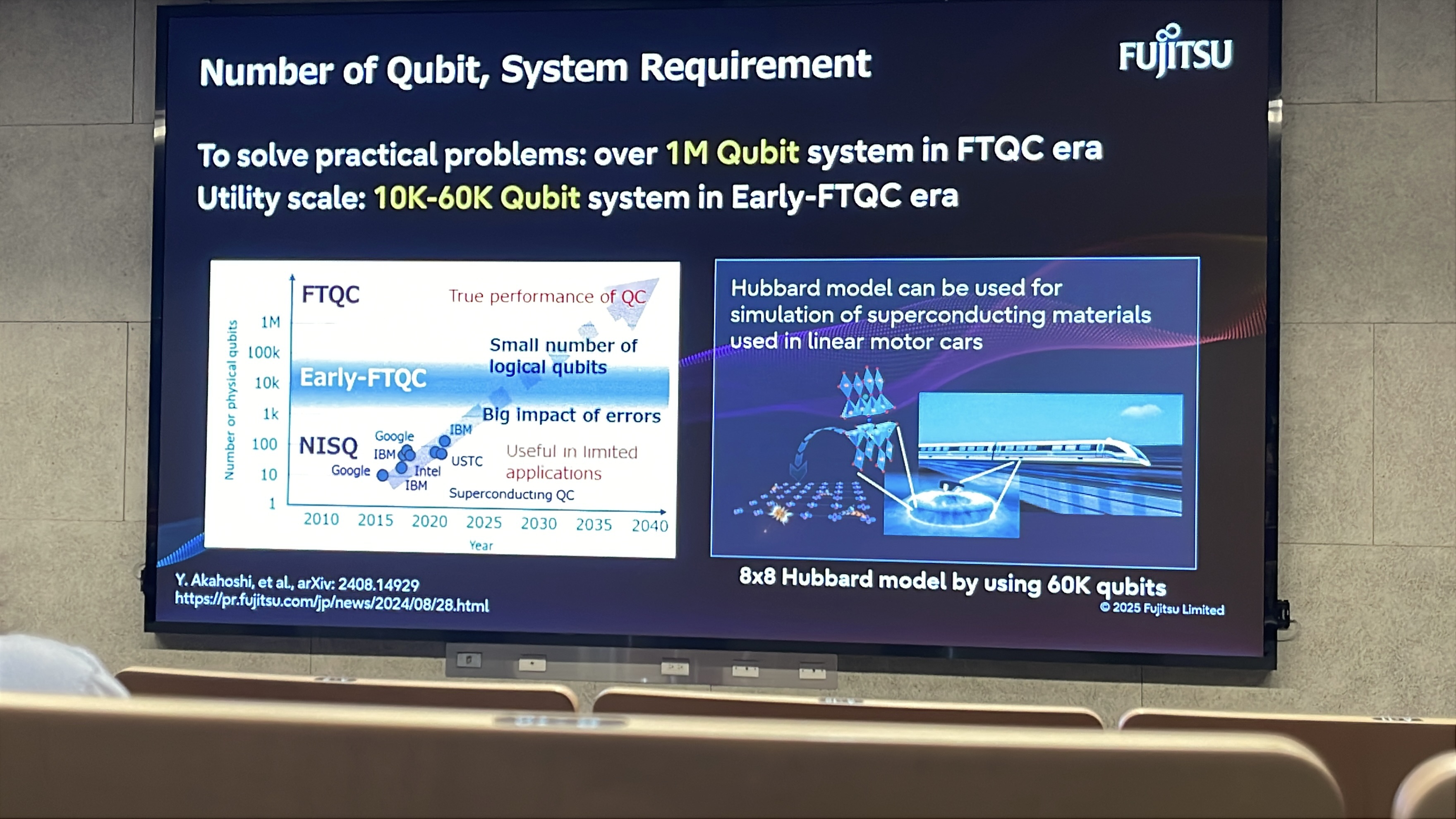
▲ FUJITSU explains the number of qubits required for Early-FTQC and full FTQC.
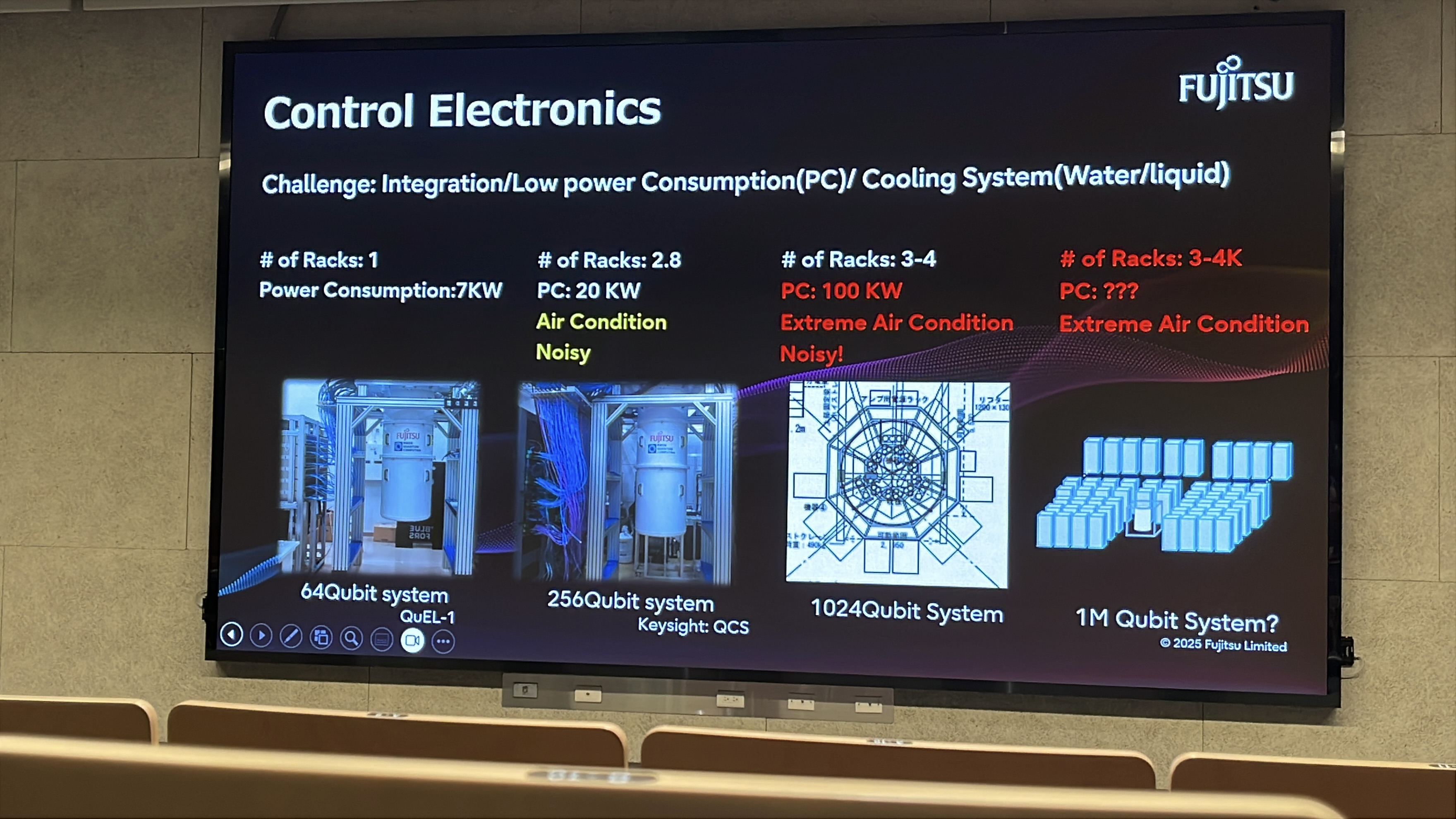
▲ The control-electronics slide lists approximately 7 kW for a 64-qubit configuration and 20 kW for a 256-qubit configuration, then discusses about 100 kW at 1,024 qubits. The million-qubit column still shows a question mark. These are the configurations and estimates presented in the talk, not universal specifications for all platforms.
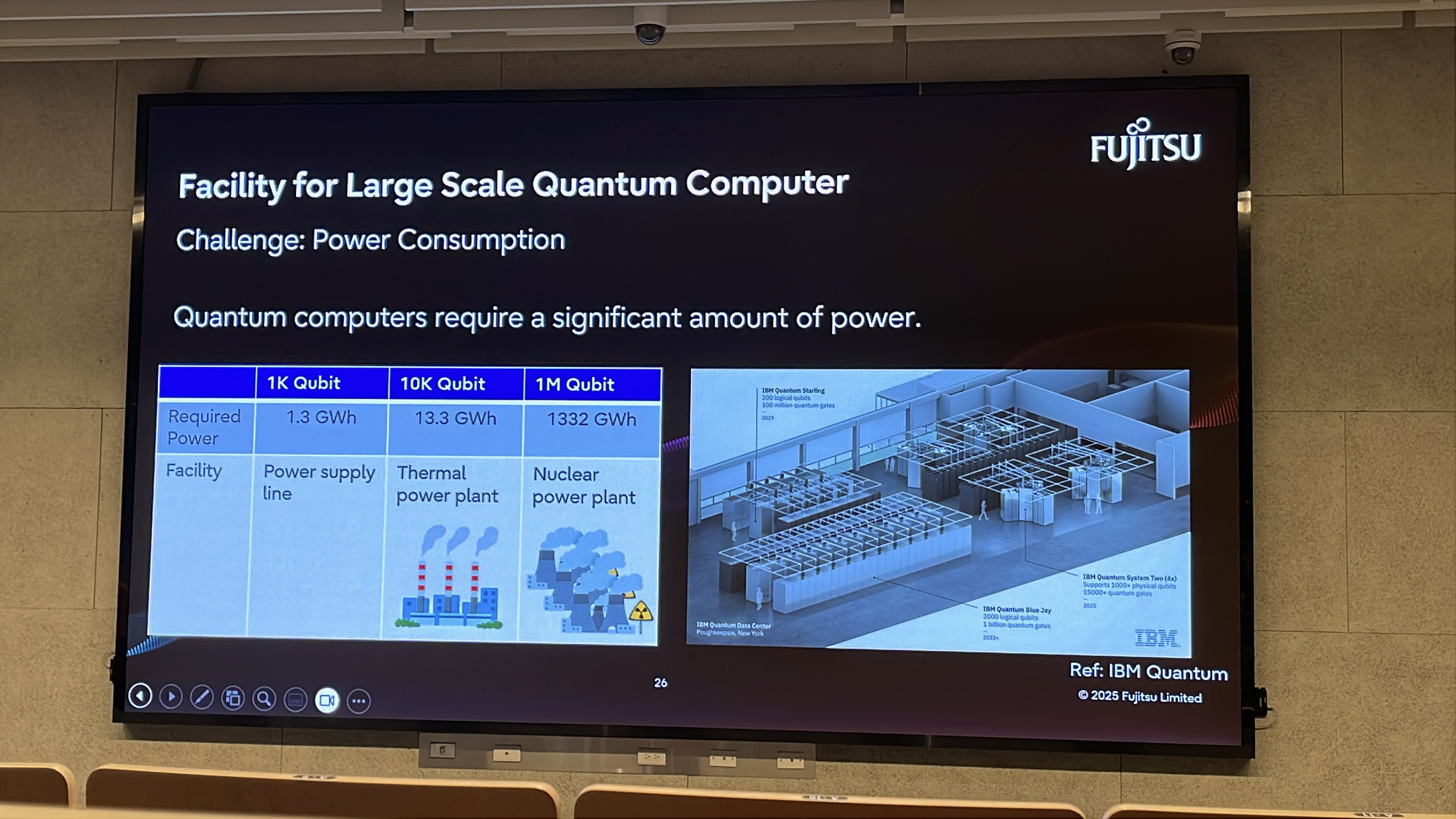
The next slide labels its row “Required Power” but uses GWh, a unit of energy. GW measures power; without the time interval over which the energy accumulates, the values cannot be converted into a required number of power plants. Infrastructure planning additionally needs operating time, utilization, and a clear boundary for cooling-system consumption.
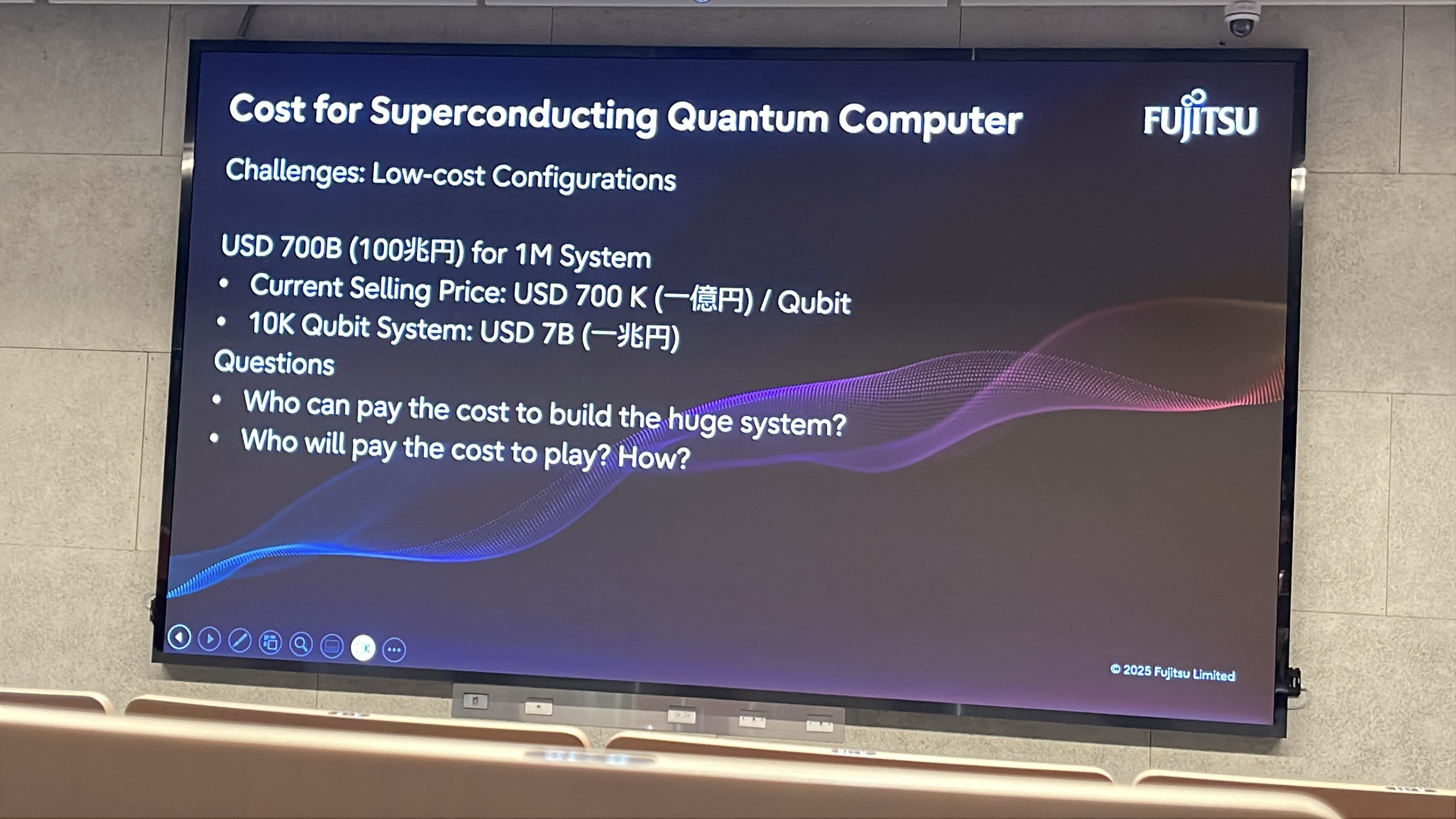
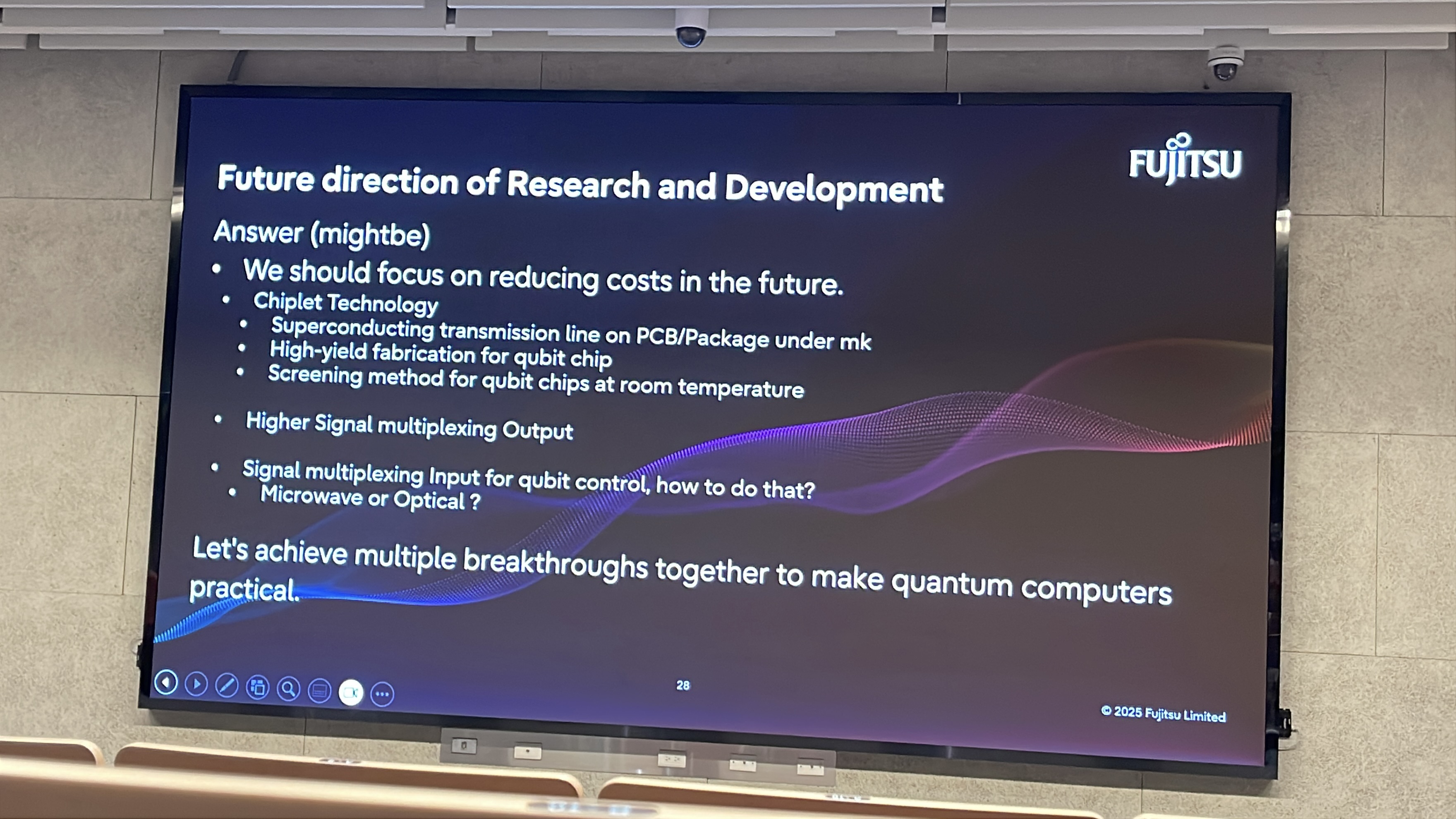
▲ Because the estimated scale of such a quantum supercomputing center is enormous, FUJITSU raises several open questions: how can the relevant infrastructure be achieved, who will help enable it, and how can the associated costs be reduced to make it more feasible?
Originally written in Chinese by the author, these articles are translated into English to invite cross-language resonance.
Connecting scale-up with calibration and operations
Fabrication variability gives individual qubits different frequencies and gate parameters. A larger processor also brings more couplings, frequency collisions, and calibration records to manage. Low-power control, dense packaging, maintainable cryogenic wiring, and automated calibration therefore belong to the same engineering problem: making a quantum processor reliably usable over time.
Sources: Workshop slides, February 6, 2026; RIKEN/Fujitsu 256-qubit announcement (2025); original STAR paper. Roadmaps and resource requirements are targets or estimates in the context of the talk.
 Peir-Ru Wang