What are Spin Qubits?
Implementations of Spin Qubits
The manifestation of quantum effects can be broadly categorized into intrinsic quantum effects, single-particle quantum effects, and statistical quantum effects:
Intrinsic Quantum Effects: These are properties inherent to particles like electrons or atoms, such as spin, spin-orbit coupling, or the polarization of photons. These properties do not depend on the external environment.
Single-Particle Quantum Effects: An individual electron or atom exhibits quantum effects under specific environmental constraints. For example, at low temperatures and within a confined potential well, when the electron's de Broglie wavelength is comparable to the characteristic scale of the well, energy quantization becomes significant. Similarly, when a material is scaled down to the nanoscale (e.g., quantum dots, nanowires, cold atoms), its properties also exhibit quantum energy levels.
Statistical Quantum Effects: A large number of electrons or atoms enter a collective quantum statistical state, where individual physical quantities lose their meaning and must be considered as a whole. Examples include superconductivity, superfluidity, Bose-Einstein condensation, lasers, ferromagnetism, as well as quasiparticle excitations in materials like phonons and excitons.
Any of the above properties can be used to create qubits for quantum computing. Semiconductor spin qubits utilize both the spin effect and the confinement effect, using a confined potential well to trap an electron and controlling its spin to store information.
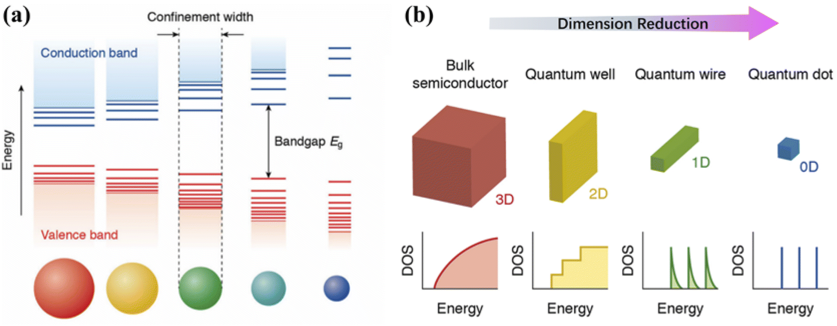
▲ As the scale of a material shrinks, quantum effects begin to manifest and energy levels become quantized.
Advancements in thermoelectric materials: optimization strategies for enhancing energy conversion
DOI: 10.1039/D4TA03666B
How are Semiconductor Qubits Realized?
As mentioned, semiconductor spin qubits use a confined potential well to trap an electron, causing it to exhibit significant quantum effects. The confinement can be achieved through material geometric confinement or artificial gate confinement. Material geometric confinement uses inhomogeneities in the material to create potential variations, while artificial gate confinement uses lithographically defined electrode patterns to apply voltages that create potential variations. These are introduced below.
| Material Geometric Confinement | Description | Gate-Assisted Confinement? |
|---|---|---|
| Dopant Impurity (0D) | A defect center is naturally formed by a dopant atom in a silicon material, for example, phosphorus doping. | Gates are used to fix the dopant's position. |
| Quantum Dot (0D) | Spherically symmetric quantum dots are self-assembled during the material growth process. | Not required. |
| Nanowire (1D) | One-dimensional nanowires can be formed through etching or crystal growth. | Gates are used for confinement along the axial direction. |
| Two-Dimensional Electron Gas (2DEG) (2D) | A free electron gas formed at a heterojunction interface. | Gates are used to define local potential wells. |
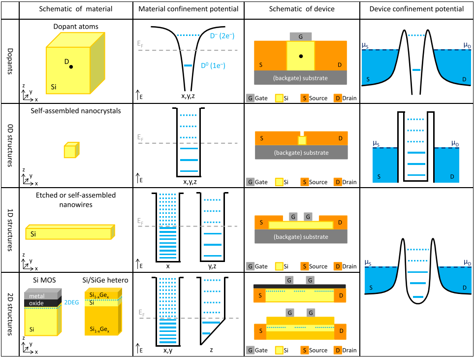
▲ Four ways to implement quantum dot qubits: impurity doping, quantum dots, nanowires, and a two-dimensional electron gas at a heterojunction.
Silicon quantum electronics
DOI:10.1103/RevModPhys.85.961
Phosphorus Doping
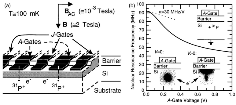
▲ Using a defect center formed by phosphorus doping to create a quantum dot.
Silicon quantum electronics
DOI:10.1103/RevModPhys.85.961
Germanium Quantum Dots
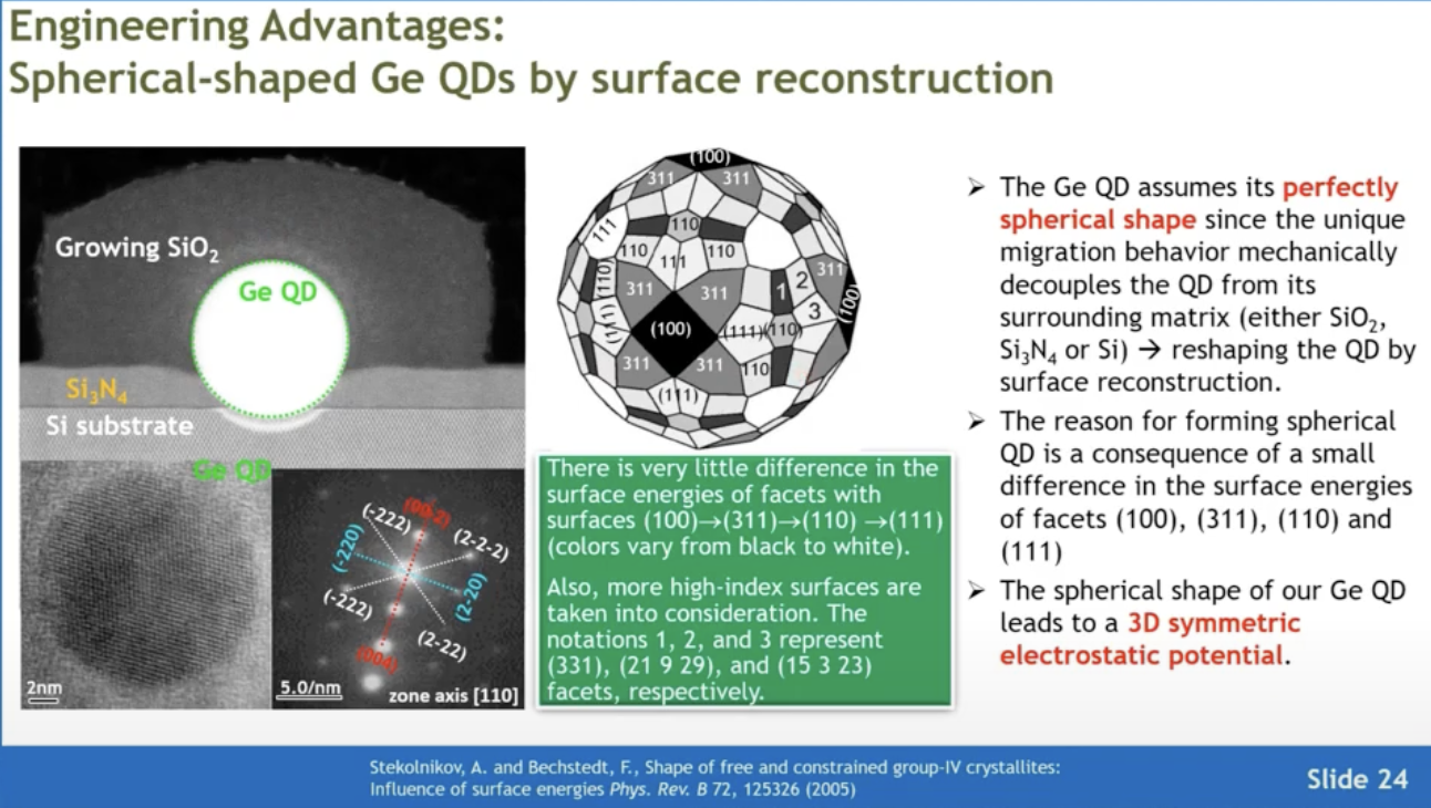
▲ Growing nanoscale spherical germanium quantum dots on a silicon material through crystal growth.
YouTube: 【2024 NYCU Electrical Engineering Project Exploration】 Introduction by Prof. Pei-Wen Li
https://www.youtube.com/watch?v=LuXsf-pWFeI&t=7s
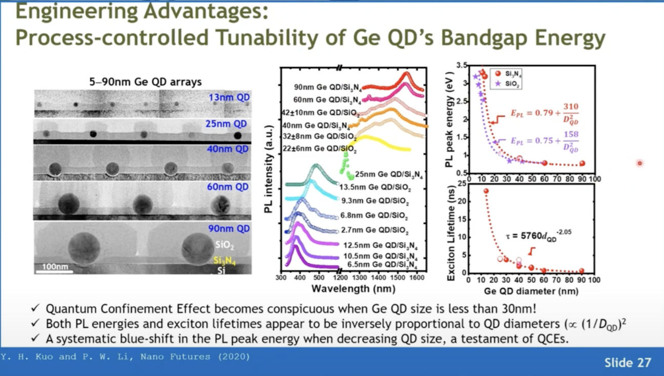
▲ The size of spherical germanium quantum dots can be controlled, which directly alters the energy gap of germanium.
YouTube: 【2024 NYCU Electrical Engineering Project Exploration】 Introduction by Prof. Pei-Wen Li
https://www.youtube.com/watch?v=LuXsf-pWFeI&t=7s
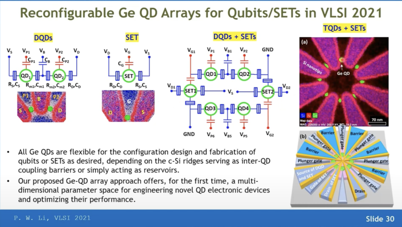
▲ Quantum dot qubits can be combined to form Double Quantum Dot (DQD) devices and can also be integrated with Single Electron Transistors (SETs).
YouTube: 【2024 NYCU Electrical Engineering Project Exploration】 Introduction by Prof. Pei-Wen Li
https://www.youtube.com/watch?v=LuXsf-pWFeI&t=7s
Nanowires
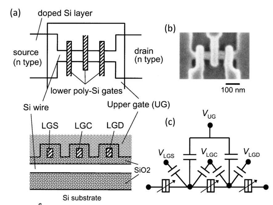
▲ Using gates on a one-dimensional nanowire to form a potential well.
Silicon quantum electronics
DOI:10.1103/RevModPhys.85.961
Gate-Defined Qubits (2D Electron Gas)
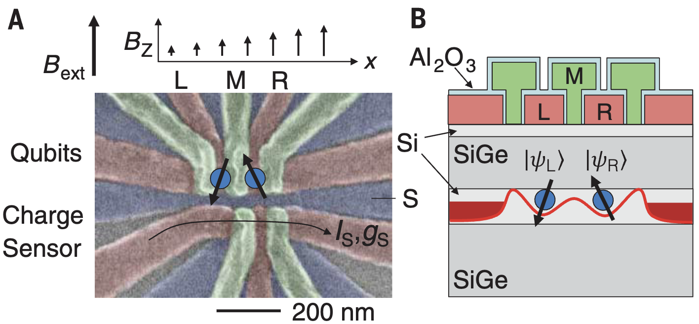
▲ The current mainstream approach for spin qubits. It utilizes the layer-by-layer deposition and etching characteristics of semiconductor fabrication. First, a heterostructure sandwich is created, for example, \(SiGe-Si-SiGe\). The middle layer then contains many freely moving electrons, forming a two-dimensional electron gas (2DEG). Gates are then fabricated on top, and the voltages applied by these gates are used to form quantum dots.
Resonantly driven CNOT gate for electron spins
DOI:10.1126/science.aao5965
Originally written in Chinese by the author, these articles are translated into English to invite cross-language resonance.
 Peir-Ru Wang