Characteristics of a Single Quantum Dot
A single quantum dot can serve as an information carrier (i.e., a qubit) or as a measurement device (i.e., a charge sensor). This article will introduce gate-defined quantum dots (Gate-based QDs).
Defining a Quantum Dot
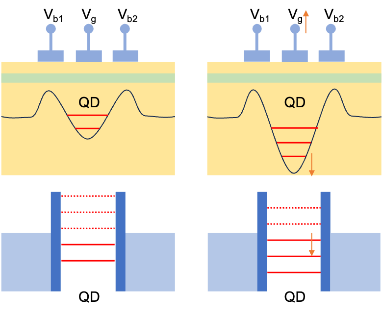
▲ A common way to define a quantum dot is by using electrodes to create potential barriers \(V_b\) and a potential well \(V_g\). The barriers cause the carriers in the potential well to have quantized energy levels, and the gate voltage \(V_g\) controls the depth of the well, thus tuning the energy levels. This defines an individual quantum dot.
Ref: Drawn by the author
Measuring a Quantum Dot
After defining a quantum dot in a material, its state can be measured using electrical transport measurements.
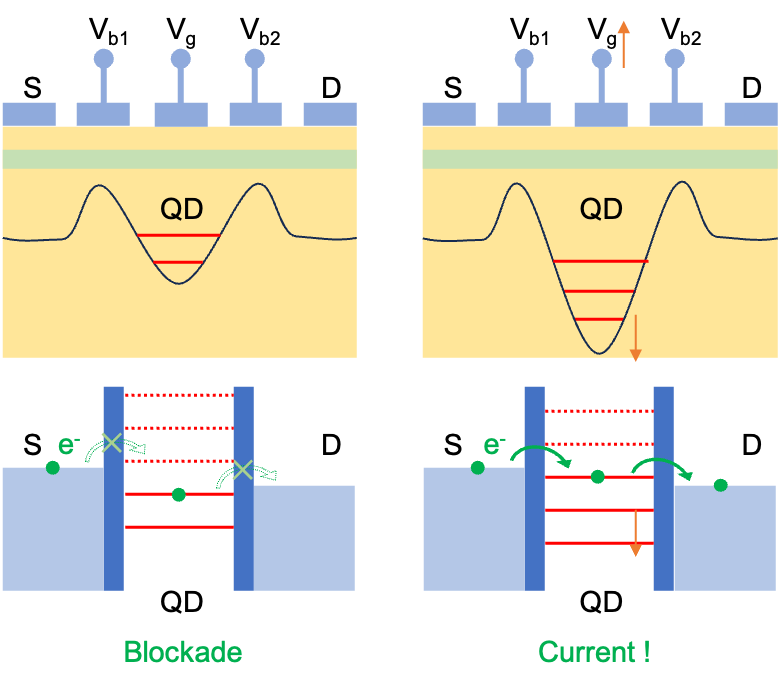
▲ To measure electrical transport, a bias voltage must be applied across two terminals (S: Source, D: Drain). This bias drives carriers to move, generating a current. By measuring the magnitude of the current, the energy level state of the quantum dot can be determined. If the quantum dot's energy level does not fall within the bias window, carriers cannot move, and no current flows. The gate voltage \(V_g\) can be used to tune the energy level into the bias window, allowing carriers to pass and thus generating a current.
Ref: Drawn by the author
Micrograph of a Single Quantum Dot
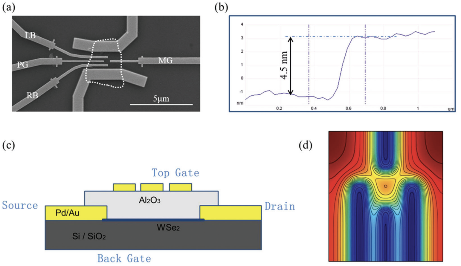
▲ A single quantum dot under an electron microscope, experimented on using six electrodes. The finer electrodes (LB, RB, PG, RG) define the confinement and potential well depth of the quantum dot. The contour plot simulation in figure (d) shows a quantum dot forming in the central region. The two thicker electrodes on the sides are used to apply bias and measure current.
A gate defined quantum dot on the twodimensional transition metal dichalcogenide semiconductor WSe2
DOI: 10.1039/c5nr04961j
Animated Simulation
Before continuing with the measurement of a single quantum dot, readers can use the animation below. By adjusting the sliders for the bias voltage \(V_s-V_d\), the gate voltage \(V_g\), and the magnetic field \(B\), you can observe whether a current is formed and how the energy levels split.
Adjust the Sliders
Measuring Energy Levels & Coulomb Diamonds
This section will introduce the extremely important Coulomb diamond measurement in semiconductor qubits.
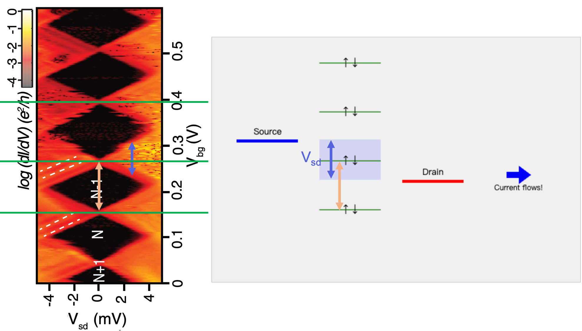
▲ By tuning the bias voltage (horizontal axis, \(V_{sd}\)) and the gate voltage (vertical axis, \(V_{bg}\)), the electrical properties of the quantum dot can be measured. Black indicates no current, while orange-red indicates current flow. Tuning the bias \(V_{sd}\) determines the size of the window where current can flow, while the gate voltage \(V_{bg}\) controls whether an energy level falls within that window. At low bias (near \(V_{sd}=0\)), current only flows when an energy level is precisely aligned within the narrow window, allowing different energy levels to be identified by tuning \(V_{bg}\). As the bias increases, the window widens, and triangular regions open up. When the bias exceeds the energy level spacing, the window will always contain an energy level, so current will always flow. The central black diamond-shaped regions are the famous Coulomb diamonds.
Ref: Transport studies of electron-hole and spin-orbit interaction in GaSb/InAsSb core-shell nanowire quantum dots
DOI: 10.1103/PhysRevB.91.161301
Originally written in Chinese by the author, these articles are translated into English to invite cross-language resonance.
 Peir-Ru Wang