Quantum Motion
2025.11.20Quantum Motion is a company focused on "silicon-based CMOS compatible" quantum computers, advocating the use of existing standard silicon processes to build scalable qubit arrays, and claims to have delivered the industry's first "full-stack silicon CMOS quantum computer." Its strategic focus is to align quantum technology with mainstream semiconductor manufacturing and packaging processes. This approach aims to maintain chip size and yield while controlling system complexity and cost, addressing the need for thousands of physical qubits in fault-tolerant quantum computing. Key R&D projects include silicon-based qubits and silicon-based Cryo-CMOS.
Products / Services
Silicon-Based Quantum Computing Platform: Qubits and quantum processor arrays built using standard silicon processes, emphasizing high integration and scalability.
Full-Stack Solutions: Claims to have delivered a "full-stack silicon CMOS quantum computer," covering everything from quantum devices to system integration.
Ecosystem and Industrial Application Collaboration: Collaborating with financial services providers to explore quantum application scenarios.
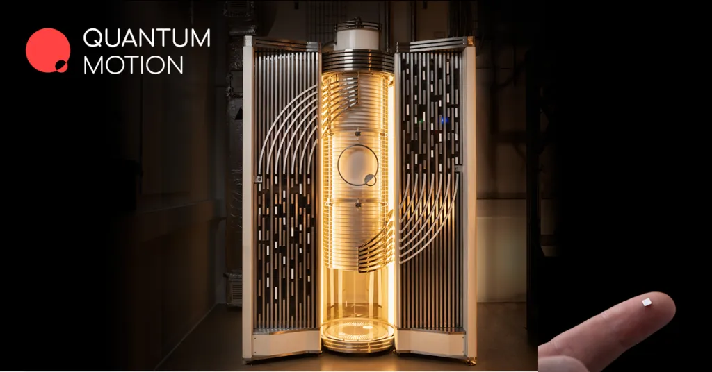
▲ Quantum computer prototype and silicon-based quantum chip launched by Quantum Motion.
Ref: https://quantummotion.com/silicons-moment-leading-the-next-wave-of-quantum-computing-in-hpc/
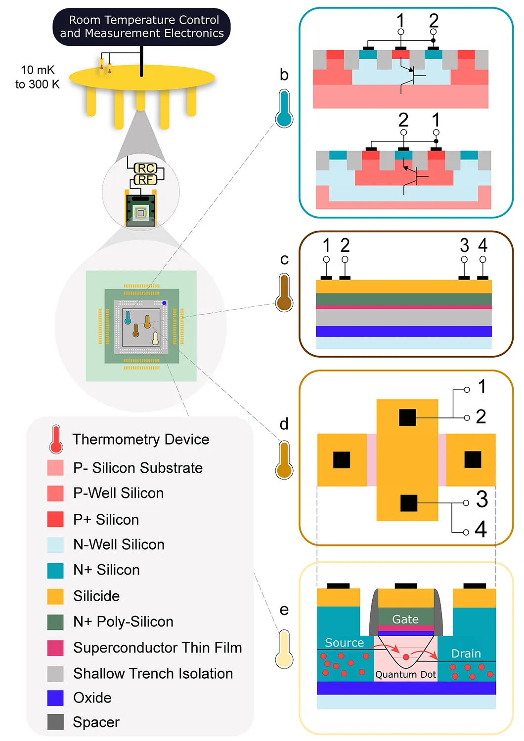
▲ The advantage of developing silicon-based Cryo-CMOS is the ability to integrate many existing semiconductor components and processes.
(b) NPN and PNP diode structures.
(c) Silicided polysilicon resistor structures, with contacts on the silicide layer, enabling 4-point measurements.
(d) Field-Effect Transistor (FET).
(e) Quantum Dot Transistor, featuring an energy level structure with sequential single-electron tunnelling.
Ref: https://quantummotion.com/cmos-on-chip-thermometry-at-deep-cryogenic-temperatures/
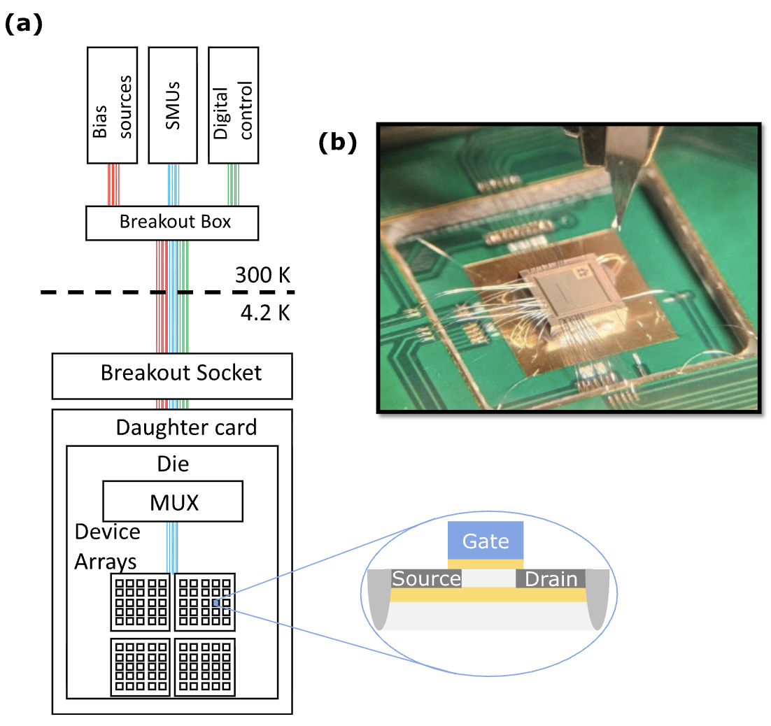
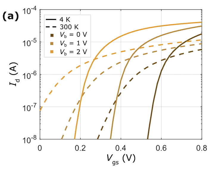
▲ Developing silicon-based Cryo-CMOS requires studying the differences in characteristics compared to room-temperature CMOS.
Ref: Method for Efficient Large-Scale Cryogenic Characterization of CMOS Technologies, DOI: 10.1109/TIM.2024.3497143
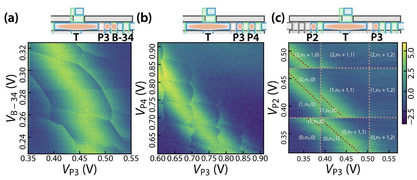
▲ Using an elongated Single-Electron Box (SEB) as a distributed sensor to measure charge stability diagrams for double quantum dots (DQD) and triple quantum dots (TQD).
(a) DQD controlled by gates P3 and B-34.
(b) DQD controlled by gates P3 and P4.
(c) TQD controlled by gates P2, T, and P3.
Ref: https://arxiv.org/pdf/2301.01650
Ref: Elongated Quantum Dots
Advantages of Elongated quantum dots / Single-Electron Box (SEB):
Diverse Geometries: No longer limited to the shape of a quantum "dot," elongated quantum dots can have diverse geometric shapes, facilitating novel and compact quantum processor layouts.
Extended Range: Through diverse geometries, the range of interaction can be extended, increasing the spacing between semiconductor quantum dots. This facilitates gate wiring and the integration of sensors with charge reservoirs, thereby offering scalability advantages.
Dual Functionality (Sensing and Coupling): Besides distributed charge sensing, they can also realize mediated coupling, extending the range of interaction between quantum dots.
Left Ref: 10.1103/PRXQuantum.2.040306
Right Ref: https://arxiv.org/pdf/2202.10516, FIG.39
Related Companies / Investors

Ref: https://quantummotion.com/
Parts of this article were generated and edited with the assistance of AI tools and reviewed by the author. Originally written in Chinese by the author, these articles are translated into English to invite cross-language resonance.
 Peir-Ru Wang